Ideas for how to fix my stacked uVia design?
dbillings , 09-07-2023, 03:11 PM
Hi everyone, this is my first post on Fedevel...
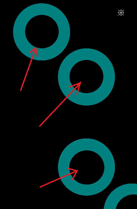
I just completed a new design with stacked uVias only to find out there is no way to generate gerbers that ensure connectivity through the via stack. Given my dielectric thicknesses it's easily manufacturable for me to stack rather than stagger my uVias. So I have two combos of stacks to get from layers 1-3 and 6-8. I used plane layers for reference ground layers on 2 and 7.


Above you can see the simple layer stack. The problem is the annular rings circled in red DO NOT EXIST on the plane layers in the way they are shown in the layer stack illustration. So the system as a whole does not support the ability to stack signal vias in order to pass signals through the ground reference layer to the first internal routing layer.
Here's an example of how I want to use the stacked uVias to escape a BGA field.

Here you can see several uVia stacks from layers 8-7 and then 7-6 to get to layer 6 shown in light blue. However, when you look at layer 7 there would need to be an annular ring around the via stack to support the connection.

All of the red circles should show annular rings of copper around the uVia stack in order to support connectivity and they don't. However there are NO DRC errors associated with these! Altium thinks they are routed successfully.
So just to show another example:

The resulting gerber for layer 7:

Just to validate, these are all definitely stacked uVia's:

I'm contending that the gerber in this case on layer 7 with the vias stacked SHOULD look something like this:
I think I drew the annular rings a little bigger than necessary but you get the idea. I'm happy to be corrected here if I'm wrong, but this is my expectation of the annular ring that would be necessary to ensure connection of the uVia's in the stack. In order to pass the signal through the layer 7-8 uVia and connect to the stacked layer 6-7 uVia, the gerber would require an annulus in copper to exist on layer 7 so the two vias can make contact with one another on an annulus. It seems that Altium plane layers are simply not usable with stacked uVia designs, and that seems to be the common consensus in the Altium developer community.
So here's the terrible thing: My design is done. Its not all that complicated but still a lot of work to fix. There is no workaround at this point. If I change the plane layers to signal layers now, Altium deletes all features that have primitives on those layers. So that means it deletes all the uVias on the whole board. If I select all the uVias and copy them to clipboard, then change the layer stack, then paste the back in to be in the same locations, it also pastes in a random plane layer into the layer stack, breaking the layer stack and essentially causing a similar rip-up. So it looks like this has wasted many weeks and I almost have to start over.
So yeah... I naively thought it would be fun to use plane layers and that they would work with stacked uVias. But my question is now that I'm in this predicament what should I do?
1. My fabricator can add an annulus back in to my gerbers for every stacked via location... But then in 2 years someone will rev the design and if their fabricator doesn't notice the problem?
2. I can rip everything up and manually re-do everything with signal layers only.
3. Complain to Altium and hope for a magic fix
4. I'm completely wrong and I should be ashamed.
Thanks for any ideas!
I just completed a new design with stacked uVias only to find out there is no way to generate gerbers that ensure connectivity through the via stack. Given my dielectric thicknesses it's easily manufacturable for me to stack rather than stagger my uVias. So I have two combos of stacks to get from layers 1-3 and 6-8. I used plane layers for reference ground layers on 2 and 7.
Above you can see the simple layer stack. The problem is the annular rings circled in red DO NOT EXIST on the plane layers in the way they are shown in the layer stack illustration. So the system as a whole does not support the ability to stack signal vias in order to pass signals through the ground reference layer to the first internal routing layer.
Here's an example of how I want to use the stacked uVias to escape a BGA field.
Here you can see several uVia stacks from layers 8-7 and then 7-6 to get to layer 6 shown in light blue. However, when you look at layer 7 there would need to be an annular ring around the via stack to support the connection.
All of the red circles should show annular rings of copper around the uVia stack in order to support connectivity and they don't. However there are NO DRC errors associated with these! Altium thinks they are routed successfully.
So just to show another example:
The resulting gerber for layer 7:
Just to validate, these are all definitely stacked uVia's:
I'm contending that the gerber in this case on layer 7 with the vias stacked SHOULD look something like this:
I think I drew the annular rings a little bigger than necessary but you get the idea. I'm happy to be corrected here if I'm wrong, but this is my expectation of the annular ring that would be necessary to ensure connection of the uVia's in the stack. In order to pass the signal through the layer 7-8 uVia and connect to the stacked layer 6-7 uVia, the gerber would require an annulus in copper to exist on layer 7 so the two vias can make contact with one another on an annulus. It seems that Altium plane layers are simply not usable with stacked uVia designs, and that seems to be the common consensus in the Altium developer community.
So here's the terrible thing: My design is done. Its not all that complicated but still a lot of work to fix. There is no workaround at this point. If I change the plane layers to signal layers now, Altium deletes all features that have primitives on those layers. So that means it deletes all the uVias on the whole board. If I select all the uVias and copy them to clipboard, then change the layer stack, then paste the back in to be in the same locations, it also pastes in a random plane layer into the layer stack, breaking the layer stack and essentially causing a similar rip-up. So it looks like this has wasted many weeks and I almost have to start over.
So yeah... I naively thought it would be fun to use plane layers and that they would work with stacked uVias. But my question is now that I'm in this predicament what should I do?
1. My fabricator can add an annulus back in to my gerbers for every stacked via location... But then in 2 years someone will rev the design and if their fabricator doesn't notice the problem?
2. I can rip everything up and manually re-do everything with signal layers only.
3. Complain to Altium and hope for a magic fix
4. I'm completely wrong and I should be ashamed.
Thanks for any ideas!

qdrives , 09-07-2023, 04:19 PM
The problem is not the gerber export.
As you can see in the 3D view, Altium does not add pads on plane layers that do not connect to the plane.
This is also mentioned here: https://designhelp.fedevel.com/forum...n-plane-layers
So first of all make sure you have a backup of your design.
Here is something to try:
1) Add 2 signal layers above the plane layer (L2) (I do assume you have stack symmetry on).
2) Add a microvia from the new layer 2 to layer 3 (in the order show in the layer stack manager)
3) Apply this to the board (save stack-up)
4) Change all microvia's to the correct new layers (Find symilar objects) --> 1-2, 2-3, 10-11, 11-12.
5) In the layer stack manager delete
5a) the microvia's to the plane layer
5b) the plane layer
5c) the third layer
5d) rename the new signal layers
6) Add the polygons on the new signal layers

Comments:
dbillings, 09-11-2023, 02:22 PM
Awww perfect Idea! I did this and it worked great, a little tedious but WAY better than re-routing all the uVia's by hand! Thanks!
WhoKnewKnows , 09-07-2023, 08:32 PM
Good luck 🤞
I'm curious to try to see if Altium can be cajoled into having pads for vias on plane layers that don't connect to that via. EG on a particular via's properties, IIRC, you can set top and bottom pad, as needed, and full stack or suthin' like that.
So, I'm thinking 🤔 What if the default via settings doesn't put on pad on a non connected plane layer, but full stack setting forces it or lets you force it?
Anyway, I'll dabble with it if I get a few spare ticks.
qdrives , 09-08-2023, 02:22 PM
@WhoKnewKnows Unfortunately, Altium skips the plane layers when selecting Full-Stack.
Comments:
dbillings, 09-11-2023, 02:23 PM
Yeah I tried everything I could think of with the Via style... I suspect the problem is fundamental to the way Altium handles plane layers.
qdrives , 09-11-2023, 02:39 PM
a little tedious
I only tried it a bit on a experiment design, not an actual fully done board.
Use our interactive Discord forum to reply or ask new questions.