Mixed-Signal PCB Design Course Preview & JLCPCB 6-Layer Assembly - Phil's Lab #16
Thank you to everyone who filled in the ´PCB Design Course Survey´ sheet. I´ve taken your comments and suggestions on board and decided to make the course based around a mixed-signal PCB (analogue + digital). We´ll be covering topics all the way from idea, to component selection, schematic creation, PCB layout, routing for minimal noise/crosstalk, grounding techniques, stackups, 4 vs 6 layer design, EMC, ESD protection, high-speed routing (length matching, impedance controlled traces), testing, and a bit of firmware and DSP algorithms!
Hopefully this´ll give a good insight into the whole design process, as well as showing many ´tricks of the trade´.
Hopefully this´ll give a good insight into the whole design process, as well as showing many ´tricks of the trade´.
Chapters:
- 00:20PCB Design Course Survey
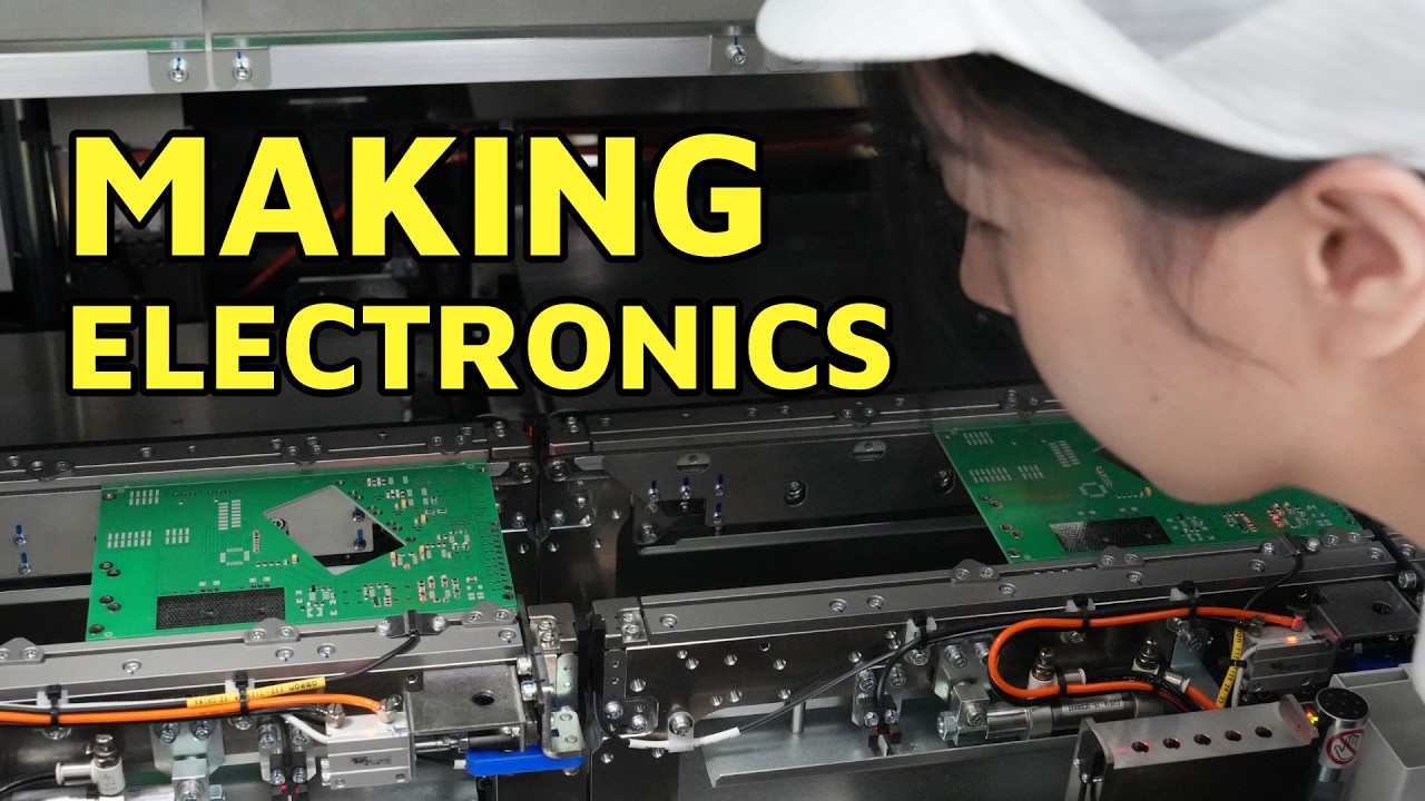
- 01:196 Layer Assembly
- 04:01Digital Section


