How to design PCB stackup
1) Leave your PCB manufacturer to design PCB stackup for you (Recommended)
Why?
- You don’t need to spend your time by designing stackup. Leave it on PCB manufacturer – they are professionals. They do it every day. Also, by doing it this way, you can work on design in parallel of handling issues with PCB stackup.
- Many times PCB manufacturer is not able to build PCB stackup designed by other company or a person outside their company. The main reason is unavailability of material used in some PCB stackups. Selection of material is the best to leave on them – they will choose stocked material.
- PCB manufacturers use different track geometry calculators and they will not guarantee track impedance if track geometry is calculated by someone else. Many times their calculated numbers and your calculated numbers will be different.
An example of email to PCB manufacturer with request for PCB stackup and track geometry.
Please suggest PCB stackup and track geometry for PCB with following parameters:
PCB Description
– 12 Layers:
L1 – Signal
L2 – GND
L3 – Signal
L4 – Signal
L5 – GND
L6 – Powers
L7 – Powers
L8 – GND
L9 – Signal
L10 – Signal
L11 – GND
L12 – Signal
Please suggest stackup.
– Required impedances:
Single ended: 50 OHMs (L1 (Ref: L2); L3, L4 (Ref: L2, L5); L9, L10 (Ref: L8, L11); L12 (Ref: L11))
Differential: 70, 90, 100 OHMs (L1 (Ref: L2); L3, L4 (Ref: L2, L5); L9, L10 (Ref: L8, L11); L12 (Ref: L11))
Please suggest geometry for impedance controlled tracks: Track width / Gap
– Used VIAs:
Through hole VIA: 0.45mm (pad)
/ 0.2mm (drill),
Start layer: L1, End layer: L12
uVIAs:
Start layer: L1, End layer: L2; 0.27mm (pad) / 0.1mm (laser drilled hole)
Start layer: L2, End layer: L3; 0.27mm (pad) / 0.1mm (laser drilled hole)
Start layer: L10, End layer: L11; 0.27mm (pad) / 0.1mm (laser drilled hole)
Start layer: L11, End layer: L12; 0.27mm (pad) / 0.1mm (laser drilled hole)
Buried VIA:
Start Layer: L3, End layer: L10; 0.45mm (pad) / 0.2mm (drill)
– Other:
Minimum track: 0.1mm / Minimum gap: 0.1mm
Board thickness: approximately 1.6mm
Board size: 40x80mm
Basic information about PCB stackups:
- PCB is build from three basic materials: Copper foil, Prepreg, Core
- Standard Copper foil thickness: 5um, 12um, 18um, 35um, 70um
- Standard prepreg thickness: 65um, 100um, 180um
- Standard core thickness: 0.15mm, 0.20mm, 0.36mm, 0.46mm, 0.56mm, 0.71mm, 1mm, 1.2mm, 1.5mm, 2.0mm, 2.4mm, 3.2mm. Core is supplied with copper foil on both sides. For some cores you need to add copper foil thickness (18um or 35um) to the core thickness.
PCB stackup examples
| Standard 4 Layer PCB stackup [mm] | Standard 6 Layer PCB stackup [mm] | Standard 8 Layer PCB stackup [mm] |
| Copper foil 0.18 prepreg 0.18 prepreg 0.71 core 0.18 prepreg 0.18 prepreg Copper foil |
Copper foil 0.10 prepreg 0.10 prepreg 0.36 core 0.10 prepreg 0.10 prepreg 0.10 prepreg 0.36 core 0.10 prepreg 0.10 prepreg Copper foil |
Copper foil 0.10 prepreg 0.10 prepreg 0.20 core 0.10 prepreg 0.10 prepreg 0.20 core 0.10 prepreg 0.10 prepreg 0.20 core 0.10 prepreg 0.10 prepreg Copper foil |
Note: If you calculate impedances for your own stackup, don’t forget about PLATING. Plating process add an additional copper (e.g. 20um) to top and bottom layer (or if you use uVIAs and buried VIAs, then also to some of the inner layers).
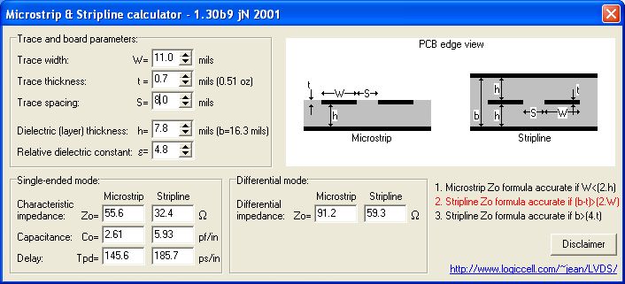
Example of Microstrip (the tracks on TOP and BOTTOM layers) impedance calculation
90 Ohms Differential / 55 Ohm Single ended for:
Track width: 11mil / Copper foil 18um (0.7mil) / Track Gap 8 mil / Dielectric thickness 2x 0.1 prepreg = 0.2mm (7.8mil) / material FR-4 (dielectric constant 4.8)
PCB impedance calculator – Single ended / Differential pair