9 Essential tips for schematic design you might not be doing
Tip 1: Import reference schematics
Why? If possible, always import schematics. If schematic is not available in a proper format which can be imported (e.g. if you only can find a pdf schematic), ask the chip manufacturer to send you board design files (usually they have Orcad files). This will save you a lot of time and minimize possible mistakes which could happen when re-drawing the schematic.Tip 2: Read Errata documents
Why? Most erratas are not important, but there are always a few which may cause you problems. You really want to double check if the listed erratas are not going to influence functionality of your board.Note: Once I used a chip with errata describing a small difference between the chip timing and timing of the official protocol. The communication between CPU and this chip failed and I had to adjust the connection.
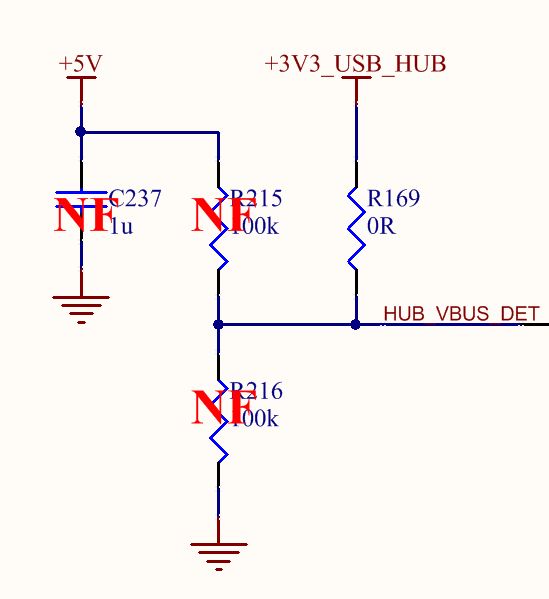
Tip 3: Mark the components which you do not want to fit by default
Why? We usually create board Variants by the end of the design (the board variants where we specify which components are going to be fitted or not fitted during mass production). However, even during schematic design process you really want to make notes about some not fitted components. In some cases, the incorrectly fitted components can damage your board (e.g. if you have option to connect part of your design to 5V or 3.3V and you fit both options at the same time).Therefore, when you are drawing schematic, decide on a default variant and mark all the unfitted components. You can for example use a text NF (Not Fitted) or some people use DNF (Do Not Fit).
Picture: An example of marking unfitted components
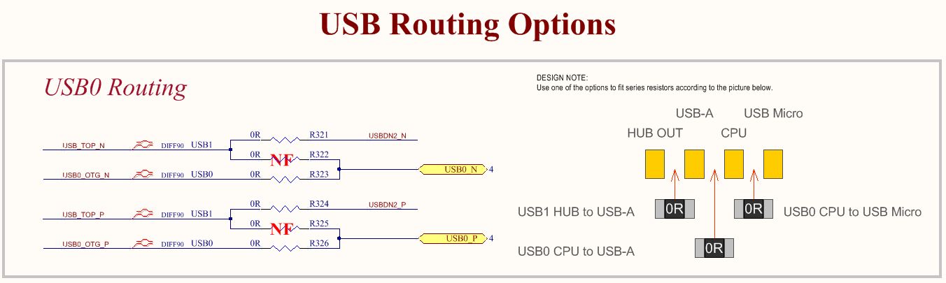
Tip 4: Use optional resistors & components
Why? Some circuits have many different options how you can connect them. Leave the optional components in the schematic. It only takes a little bit of space on the PCB, but it can add support for very specific custom configurations, it can help you a lot if you need to tweak something or if something is not working as you expected.Note: Using a lot of optional components is actually one of the secrets why many of our boards can go into mass production as Version 1 Issue 1. We leave a lot of options in the schematic and in the PCB, we do a lot of testing and we fit / unfit the components on the prototype the way it works reliably and well. The prototype then doesn’t need any PCB redesign, it goes directly to mass production.
Picture: Optional resistors on USB routing
Tip 5: If you are not sure, add bypass options
Why? Sometimes you may not be 100% sure if the circuit will work exactly as you are expecting. In this case, add a bypass option, so you can simply go around the circuit, your board will not support that specific feature, but you still can do mass production and sell it without redesigning the board.Tip 6: When you are not sure if put something into your schematic, add it there
Why? This will speed up the development a lot. You can always remove it later. Do not spend time by thinking and considering if put something (a circuit, component, feature, connector, …) into your schematic or not. Just put it there. Later, when you will be doing preliminary placement and you see, that not everything is going to fit on the board, then you can re-consider what you would like to remove.Note: Just waiting for approvals may delay your project for months (e.g. you have to ask your boss, your boss has to ask your client, the client has to ask their engineers, ….). So, when you are drawing a schematic, simply put everything into it and later, on one meeting only, go through the placement and if it doesn’t fit, decide what you are going to remove. This way, you do not have to wait weeks for answers about every connector or feature.
If you are doing the project for yourself, you also do not want to spent time by thinking “Shall I put it there or Not?”, put it there and move to the next thing. It’s just a schematic.. If needed, you can always remove it later.
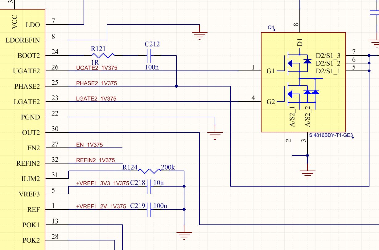
Tip 7: Name every important net in your schematic, even if it connects only 2 pins on the same page
Why? It is very helpful during PCB layout. You immediately know what net you are routing. And some nets are very important. Based on the net name, you may need to do the track very short, or wide or route it away from all the other signals, ….Note: When I was starting with hardware design, I was always wondering why in some schematics they place net names also on simple 2 pin connections. Now I know, they do it, because it’s useful.
Picture: Example of naming simple nets in a power supply design
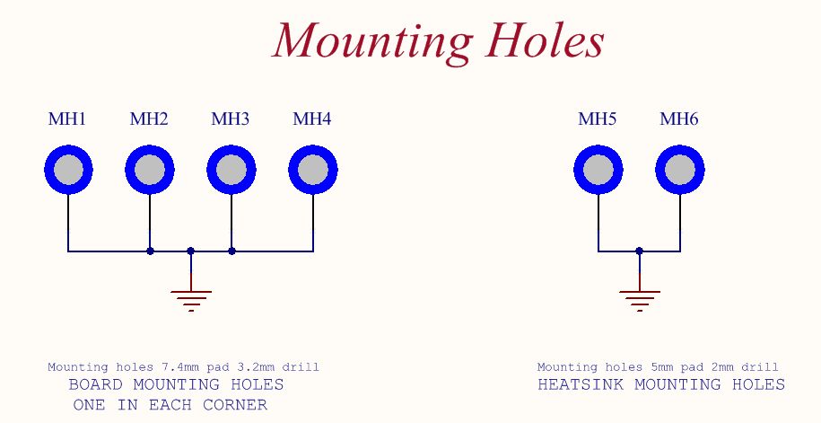
Tip 8: Add “PCB only” components into your schematic (mounting holes, fiducials, …)
Why? When you synchronize Schematic and PCB, you would like to have “No difference” between them. Also, some components such mounting holes need to be connected to a net e.g. GND. Some people create these components manually in PCB only, but you can easily create a mounting hole schematic symbol, create the “footprint” – in the case of mounting hole it is a simple pad, add this to your schematic and connect it to GND. It may look complicated, but this way you are 100% sure, the mounting holes are included in your PCB and correctly connected. Do the same for other components e.g. fiducials.Picture: Mounting holes in schematic
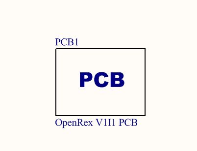
Tip 9: Add “BOM only” components into your schematic (PCB, spacers, heatsink, …)
Why? It’s going to save you a lot of time and it will help with purchasing a lot.Note: Before I started including these things in BOM, I regularly received questions such what heatsink I should order, what spacers we are using, where I can buy the screws for the board, … and every time I had to go on the component supplier website and look for the order number. Now I include everything in the schematic and when they are building a board, they immediately see from the BOM what screws, heatsink or spacers they should buy.
In your schematic you may want to include also things like PCB name and version (so, your purchasing department know from the BOM what PCBs they should order to build the board) and you may want to include also Firmware and description with information what chips have to be flashed. When someone will be preparing material for production, they will know, that they should send out files with particular software / firmware and the assembly house can see from the BOM, that they should flash the firmware into the chips.
Picture: PCB schematic symbol